Seven Segment Decoder
Problem #313
Tags:
logic
challenge
practical
special
This task has a Challenge attached.
You may
View Stats
or read a Help on Challenges.

"Two Steves" when they were young and had great plans
While browsing the history of Apple Inc. company, I found curious fragment about one of the projects
Steve Jobs and Steve Wozniak were participating in. While working for Atari on the Breakout video game,
Jobs had managed to reach agreement on being paid $100 for every chip eliminated from the project design.
We understand that it was a time when video games were often not programmed, but rather built from handfuls
of logic chips and other electronic parts. Jobs really delegated the work to Wozniak who was a kind of
electronic design genius already.
This problem is somewhat unusual - you are to feel yourself a bit more like electronics designer rather than programer. Almost to try yourself in the role of Steve Wozniak. Though we choose some much simpler goal.
You may know this popular kind of display, where numeric digits are formed by combination of 7 lines - called Seven-Segment Display. Generally these 7 lines or bars have dedicated "names", when addressed in schematic, let me show this:
 aaaaaa
f      b      for example
f      b
f      b      digit "4" is represented by b,c,f,g segments
 gggggg
e      c      digit "2" is represented by a,b,d,e,g segments
e      c
e      c      and so on
 dddddd
Generally any electronic circuit dealing with numbers will represent them in binary (or BCD) form - i.e.
there are 4 bits (or rather 4 wires, inputs), let's name them x3, x2, x1, x0 - and for example value
5 which is 0101 in binary, is represented by wires x2 and x0 having logic 1 while others
having logic 0.
Now the task is to create decoder - e.g. logic function (or rather electronic design) which takes
these x3, x2, x1, x0 as input and produce proper digit shapes with a, b, c, d , e, f, g outputs. For
example to display 6 we got x2 and x1 set to 1 (others being 0) and this should be converted
to c, d, f, e, g set to 1 (note we want "short-tailed" 6 and 9 shapes).
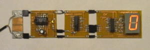
Please use the digit shapes just as in this demo. This gadget cosists of modules created by my students back in 2016. It consists of square pulses generator, decimal counter, seven-seg decoder and at last display itself. Particularly decoder/display module was designed and soldered by Olesya K.. It uses somewhat unusual shapes for "6" and "9" - please follow this pattern!
As usually, electronics designer has not every imaginable logic functions in form of chips. We are going to
deal with NAND and NOR functions only (they are AND, OR with the output inverted) - these are perhaps
the most popular in hardware logic designs.
You are to describe solution in very primitive language, like this:
; comments start with semicolon
m = nand(x1, x0)
z2 = nor(x3, m)
y = nand(x2)    ; simple inverter
r = nand(x0)
a = nand(y,z2,r)
You see, every line defines "wiring" of single logic block.
On the left is the name for some new signal which gots its value by applying logic function nand or nor to
some other signals (inputs to given block). Nested functions are not parsed, so use "intermediate" signals
naming them with a letter and, optionally, single digit.
Remember that signals x0...x3 and a...f have special meaning, being treated as inputs and outputs.
No input or answer boxes are needed for this problem. However here is interactive visualization of how your code (or your "design") works, above the solution area - please notice the line hinting about errors below it.
Chips counting
This task is in a "challenge" format, so that it is not possible to view peer's solutions (supposedly this doesn't make much sense). However chip count doesn't affect score, which is constant - the problem just needs to be solved. This is purely for amusement and as motivation to spend some more time on optimizing your design. The challenge comment will tell how many chips your design is using.
We assume real chips of 74xx series
are used. They usually have more than 10 pins so generally several small logic blocks are packed in single
chip. Particularly we shall use
quad 2-inputNANDs and NORs (e.g. 74x00, 74x02)triple 3-inputNANDs and NORs (e.g. 74x10, 74x27)double 4-inputNANDs and NORs (e.g. 74x20, 74x29)single 8-inputNANDs and NORs (e.g. 74x30, 74x4078)
Note that for example 5-input function is implemented by 8-input chip. Similarly if we need single-input
inverter, we need to use 2-input block anyway (despite dedicated inverter chips exist).
All unused pins are usually tied to one of the power lines (to provide either constant 0 or 1).
Also note that chips contain blocks of the same type, there are no chips with mixed nands and nors.
Let's regard the abstract example given above. We have 4 NAND blocks, largest of them with 3 inputs, and
also lonely nor block. It looks we'll need 3 x 3-input NAND chip to pack 3 of the NAND functions and
inevitably one more NAND chip (for remaining one NAND block) - and at last dedicated NOR chip. Two last chips
could be with any input configuration and seem to be used quite inefficiently.
But we can do better, just replace y = nand(x2) with nor (which makes no difference) - and only two
chips are needed!